무엇을 해야하는지부터 우선 제대로 확인하자.
컴퓨터와 fpga보드를 이더넷으로 연결한다.
(현재 나는 컴퓨터의 포트가 부족해서 공유기에 연결했다.)
그들간의 주소를 MAC, PHY를 통해 정확히 지칭해주어야 한다.
FPGA 보드내에 data를 PC로 전송하는 것으로 하자.
data는 다음과 같이 Hello World!!! 를 사용하자.
{"H","e","l","l"}
{"o"," ","W","o"}
{"r","l","d","!"}
{"!","!","\r","\n"}

인터넷 설정을 조금 살펴보자.
ASUS 공유기를 Source로 ASRock 마더보드를 Destination으로 움직인다.
하지만 ip와 관련해서는 자동 ip생성을 하고 있어, 고정 ip설정을 해주어야 할까 싶다.
(하지만 이 작업을 수행하는 과정에서 기존 설정된 nas의 ip설정이 흔들릴 수 있을듯하다.)
내 컴퓨터에서 ip를 바꿈으로 인해서 문제가 될만한 부분이 없을지 점검하고, 이 부분 설정부터 하도록 하자.


Frame 2486: 60 bytes on wire (480 bits), 60 bytes captured (480 bits) on interface \Device\NPF_{BF623DAC-5CB9-4DA5-9C62-EE3A300B81A9}, id 0
Ethernet II, Src: ASUSTekC_ab:97:b8 (f0:2f:74:ab:97:b8), Dst: ASRockIn_61:9a:e4 (a8:a1:59:61:9a:e4)
Destination: ASRockIn_61:9a:e4 (a8:a1:59:61:9a:e4)
Address: ASRockIn_61:9a:e4 (a8:a1:59:61:9a:e4)
.... ..0. .... .... .... .... = LG bit: Globally unique address (factory default)
.... ...0 .... .... .... .... = IG bit: Individual address (unicast)
Source: ASUSTekC_ab:97:b8 (f0:2f:74:ab:97:b8)
Address: ASUSTekC_ab:97:b8 (f0:2f:74:ab:97:b8)
.... ..0. .... .... .... .... = LG bit: Globally unique address (factory default)
.... ...0 .... .... .... .... = IG bit: Individual address (unicast)
Type: IPv4 (0x0800)
Padding: 000000000000
Internet Protocol Version 4, Src: 121.53.218.30, Dst: 192.168.50.248
Transmission Control Protocol, Src Port: 443, Dst Port: 52848, Seq: 232099, Len: 0
그리고 아직 확인이 안된게, 공유기 뒤에서 여러개의 포트가 꽂혀 있는데
거기서의 src, dst 관계도 확인이 아직 된것이 아님을 알자.
그리고 모프로젝트에서 '실행'과 관련된 부분을 보자.

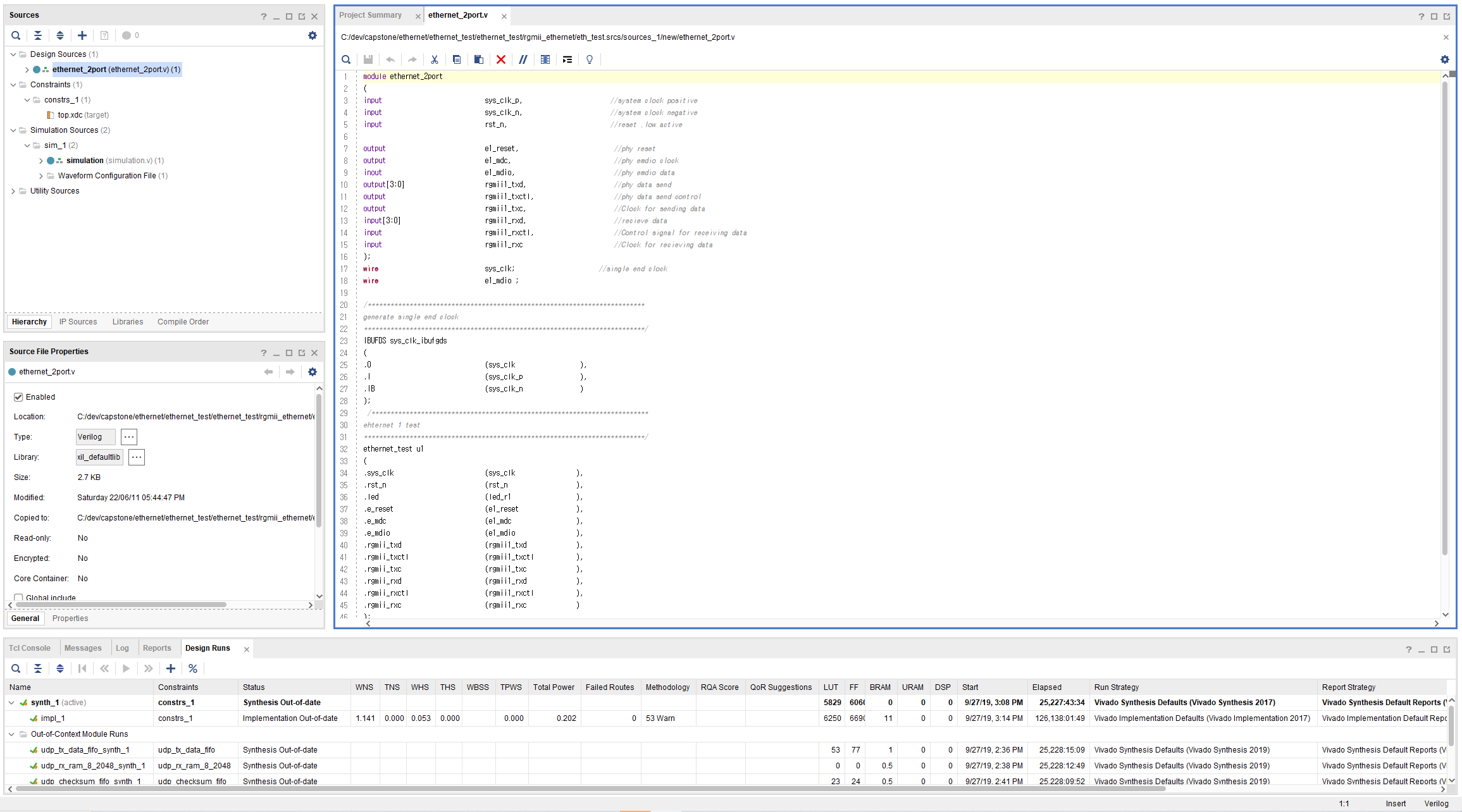
프로젝트를 2022 ver 로 업데이트 해오는 과정에서 뭐가 깨진것 처럼 보인다.
그리고 어차피 원래 있던 RTL 프로젝트 그대로 못쓴다
내 보드랑 여기 보드랑 다르다. 구성을 다시하면서 클락같은 부분들까지 다 맞춰주어야 한다.
(차라리 ti 프로젝트를 끌고와서 그걸 수정하는게 빠를듯싶다.)
이 프로젝트가 어떤 구성을 기반으로해서 etherenet_test 모듈과 연결되는지를 이해해야한다.

다음 모식도 참고하면 이해가 될듯한데
이 모식도가 생성된 곳을 찾아가보자.

RGMII에 대해 알아야하는데
이건 MII - GMII - RGMII 형태로 진화했다.
interface types (MII, GMII, RGMII) advantages and disadvantages – Ethernet Experiment – FPGA Board for Beginner – Experime
Experiment 14 Ethernet Experiment 14.1 Experiment Objective Understand what Ethernet is and how it works Familiar with the relationship between different interface types (MII, GMII, RGMII) and their advantages and disadvantages (our development board uses
fraserinnovations.com

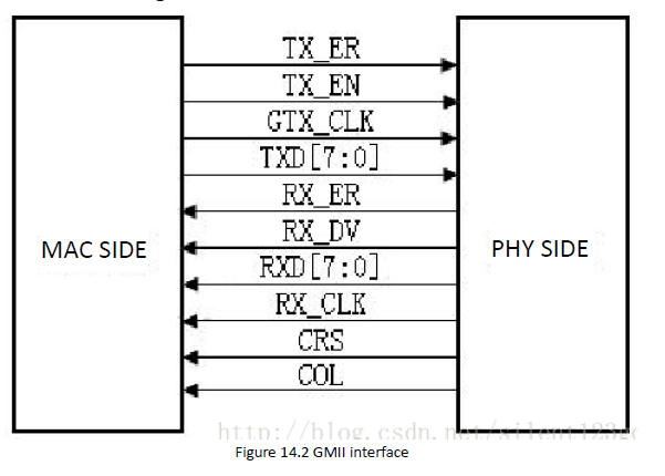

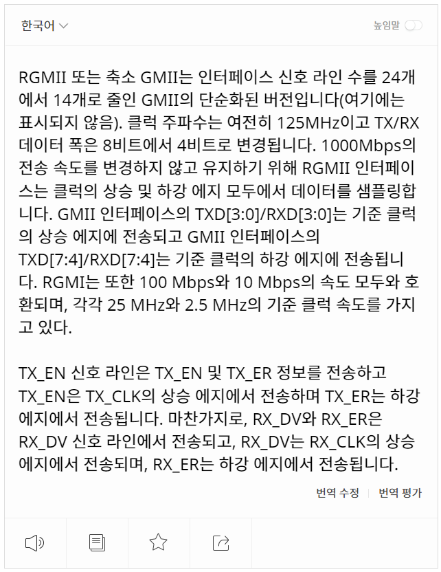
RGMII는 Reduced GMII이다.
RGMII, or reduced GMII, is a simplified version of GMII, which reduces the number of interface signal lines from 24 to 14 (COL/CRS port status indication signals, not shown here), the clock frequency is still 125MHz, and the TX/RX data width is changed from 8 to 4 bits. To keep the transmission rate of 1000 Mbps unchanged, the RGMII interface samples data on both the rising and falling edges of the clock. TXD[3:0]/RXD[3:0] in the GMII interface is transmitted on the rising edge of the reference clock, and TXD[7:4]/RXD[7:4] in the GMII interface is transmitted on the falling edge of the reference clock. RGMI is also compatible with both 100Mbps and 10Mbps rates, with reference clock rates of 25MHz and 2.5MHz, respectively.
The TX_EN signal line transmits TX_EN and TX_ER information, TX_EN is transmitted on the rising edge of TX_CLK, and TX_ER is transmitted on the falling edge. Similarly, RX_DV and RX_ER are transmitted on the RX_DV signal line, and RX_DV is transmitted on the rising edge of RX_CLK, and RX_ER is transmitted on the falling edge.
(그나저나 발견한건데 이 블로그 좋다.)
https://fraserinnovations.com/category/fpga-tutor/
Ubuntu Network Connections Guide in FPGA Board Development Environment
fraserinnovations.com
깃헙에서 비슷한 파일을 찾긴했다.
https://github.com/andres-mancera/ethernet_10ge_mac_SV_UVM_tb
GitHub - andres-mancera/ethernet_10ge_mac_SV_UVM_tb: SystemVerilog-based UVM testbench for an Ethernet 10GE MAC core
SystemVerilog-based UVM testbench for an Ethernet 10GE MAC core - GitHub - andres-mancera/ethernet_10ge_mac_SV_UVM_tb: SystemVerilog-based UVM testbench for an Ethernet 10GE MAC core
github.com
알릭스 교육부서에서 만든 파일같다.
芯驿电子科技(上海)有限公司
XILINX官方合作伙伴 FPGA高端培训机构 技术人才培养基地
www.alinx.com
=====
22/08/15
실수로 NAS에 디렉토리가 있던게 문제였다.
NAS에 있던걸 C:// 디렉토리로 옮겼다. 그랬더니 프로젝트가 정상적으로 보인다.
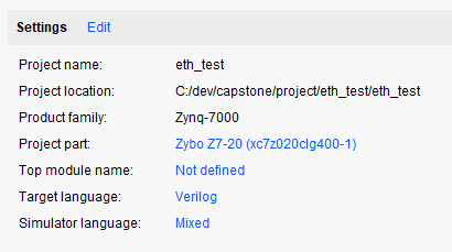
이건 Zybo 보드가 기준인 프로젝트가 아니므로
Zybo Z7-20을 기준으로 하는 신규 프로젝트를 생성해준다.
src 파일들 복붙해주기.
by 'copy source into project'
그러나 이전 프로젝트에 대한 이해도 부족으로 인해서
가져오는 과정에서 여러 충돌 발생. 모두 삭제.

가장 깔끔한 방법은
수작업으로 가져오는 것일것으로 판단.
수행.
그런데 중간에 lock 걸려있는 ip 같은 것들이 있어서
단순히 코드 복사오는 것으로는 막히는 지점이 생긴다. ㅠ

import를 잘해보자.
아 근데 import를 하지 말고
그냥 ethernet 사용했던 프로젝트를 보는게 편하지 않을까.
어차피 다른 프로젝트들도 다른 방법으로 잘 해낼텐데
굳이 이 source project에 집착해야할까.
다시 잠시 다른 방법을 찾아본다.
===
출처: https://xilinx.tistory.com/entry/fpga를-이용한-고속-데이터-전송방법-설계-aurora-ethernet-iserdes-oserdes [KIM HYUK, XILINX EMBEDDED SFAE, Zynq:티스토리]
===
https://digilent.com/reference/programmable-logic/zybo-z7/reference-manual
Zybo Z7 Reference Manual - Digilent Reference
digilent.com
10 Ethernet
The Zybo Z7 uses a Realtek PHY to implement a 10/100/1000 Ethernet port for network connection.
One of several Realtek PHY parts may be loaded on your board, depending on the revision of the board. To find out which part is loaded, check the PCB revision on the underside of the PCB. These devices are not functionally equivalent and may require changes to user applications, depending on the board support package (OS, drivers, and libraries) used. The table below lists the possible load options, and a non-exhaustive list of the differences between these two PHY devices is presented at the end of this section.
Table 10.1: Ethernet PHY part loaded
| RTL8211E | < D.0 |
| RTL8211F | ≥ D.0 |
The PHY connects to MIO Bank 501 (1.8V) and interfaces to the Zynq-7000 AP SoC via RGMII for data and MDIO for management. The auxiliary interrupt (INTB) and reset (PHYRSTB) signals connect to PL pins to be accessed via EMIO. The connection diagram can be seen on Figure 10.1.
After power-up the PHY starts with Auto Negotiation enabled, advertising 10/100/1000 link speeds and full duplex. If there is an Ethernet-capable partner connected, the PHY automatically establishes a link with it, even with the Zynq not configured.

Figure 10.1. Ethernet PHY signals
Three status indicator LEDs, labeled “10”, “100”, and “1G” near the RJ-45 connector indicate both status and link state of the three connection speeds. Table 10.1 shows the default behavior.
| Designator | State | Description |
| 10 | Steady on | Link Up at 10 Mbps |
| Blinking | Transmitting or Receiving | |
| 100 | Steady on | Link Up at 100 Mbps |
| Blinking | Transmitting or Receiving | |
| 1G | Steady on | Link Up at 1000 Mbps |
| Blinking | Transmitting or Receiving |
Table 10.1. Ethernet status LEDs
Prior to revision D.0, only two status indicator LEDs were used (“LINK” and “ACT”). Check the dropdown below to determine their behavior.
Revision < D.0 LED BehaviorThe Zynq incorporates two independent Gigabit Ethernet Controllers. They implement a 10/100/1000 half/full duplex Ethernet MAC. Of these two, GEM 0 can be mapped to the MIO pins where the PHY interfaces. Since the MIO bank is powered from 1.8V, the RGMII interface uses 1.8V HSTL Class 1 drivers. For this I/O standard an external reference of 0.9V is provided in bank 501 (PS_MIO_VREF). Mapping out the correct pins and configuring the interface is handled by the Zybo Z7 Vivado board files.
Although the default power-up configuration of the PHY might be enough in most applications, the MDIO bus is available for management. The PHY is assigned the 5-bit address 00001 on the MDIO bus. With simple register read and write commands, status information can be read out or configuration changed. The Realtek PHY follows industry-standard register map for basic configuration.
The RGMII specification calls for the receive (RXC) and transmit clock (TXC) to be delayed relative to the data signals (RXD[0:3], RXCTL and TXD[0:3], TXCTL). Xilinx PCB guidelines also require this delay to be added. The PHY is capable of inserting a 2ns delay on both the TXC and RXC so that board traces do not need to be made longer.
On an Ethernet network, each node needs a unique MAC address. The Quad-SPI flash memory is programmed with a 48-bit globally unique EUI-48/64™ compatible identifier during manufacturing. Due to changes in which flash part is loaded on the Zybo Z7, accessing the MAC address differs slightly depending on which revision of the board you have. For revisions prior to F.0, the MAC address is contained in the one-time-programmable (OTP) region of the Quad-SPI flash. The OTP address range [0x20;0x25] contains the identifier with the first byte in transmission byte order being at the lowest address. For revisions after and including F.0, the MAC address is contained in the security registers and needs to be read out using the Read Security Registers (48h) command from the address range [001000h;001005h]. The byte order is the same as in older revisions, ie. the first byte in transmission byte order is at the lowest address. Refer to the Flash memory datasheet that is associated with the chip loaded on the board (see the Quad SPI Flash section for more details) for information on the commands required to access these memory regions.
When using Petalinux, regardless of which flash memory is loaded, reading the MAC address is automatically handled in the U-boot boot-loader, and the Linux system is automatically configured to use this unique MAC address. The identifier is also printed on a sticker found on the top-side of the Zybo Z7 right next to the mode jumper (JP5) and above the headphone output jack.
For getting started using the ethernet port in a bare-metal application, Xilinx provides a lwip TCP/IP stack that can be automatically generated in Xilinx SDK along with an echo server example. When using the Zybo Z7 with a Petalinux generated embedded Linux system, the ethernet port will automatically appear as a network device typically named eth0. See the Petalinux and Xilinx SDK documentation for more information.
For more low-level information on using the Zynq-7000 Gigabit Ethernet MAC, refer to the Xilinx Zynq Technical Reference Manual.
Differences between the RTL8211E and RTL8211F:
-
PHYSR1 (PHY Specific Status Register 1) at Page 0xA43, Address 0x1A vs. PHYSR at Address 0x11. Register field layout also differs. Affected functionality includes auto-negotiated speed, duplex and link detection.
-
INSR (Interrupt Status Register) at Page 0xA43, Address 0x1D vs. INSR at Address 0x13. Register field layout also differs. Affected functionality is interrupt detection.
-
INER (Interrupt Enable Register) power-on defaults to only the PHY Register Accessible Interrupt being enabled vs. all interrupt sources enabled. Interrupt sources must now be explicitly enabled, if required.
-
Power-on sequencing requirements changed. The RTL8211F now regulates its own core voltage, as its internal regulator cannot be turned off. The 1.8V I/O voltage sequencing requirements forced all I/O circuitry in bank 501 (Ethernet, USB, UART, SD) to be separated from the main 1.8V board supply by a load switch. This I/O supply is now the last in the sequence to power-on. The board power-on reset circuitry required to be changed as well. Power-on now takes more time.
-
Power-on core logic ready time 100 ms vs. 20 ms. The RTL8211F reserves a 100 ms window after power-on that is not being used for now. The only register access allowed in this window is Page 0xa46, Reg. 20, bit[1]=1 (PHY Special Config Done), to skip this window and enter normal operating state. Otherwise, the PHY will do it automatically when the wait period ends. Entering normal operating state is signaled by the ETH_INT_B interrupt. This behavior affects only very short boot time applications, which have been explicitly optimized for this purpose. Such applications must make sure they monitor the PHY interrupt and do not access any registers other than the one stated above before the Special Config Done even arrives. The typical boot time of a small non-optimized stand-alone application from the QSPI flash is 86 ms from the de-assertion the PS_POR_B signal. The PS_POR_B delay was increased and the PHY is now taken out of reset ahead of the Zynq. Therefore, without specific boot time optimizations, the RTL8211F is guaranteed to be ready by the time the software needs it.
-
Three PHY status LEDs vs. two. The Link and Activity LEDs have been replaced by one LED for each link speed that integrate link and activity. These are now labeled “10”, “100”, and “1G”.
Suggested embedded software work-arounds depending on the board support package:
-
Stand-alone environments are expected to be using Xilinx’s lwip library with built-in PHY support for the RTL8211E. This will need to be replaced by a modified library that adds support for the RTL8211F. The patched library is published on Digilent’s Github page: Patched Library. It is expected to be upstreamed to Xilinx in a future Vitis version.
If the ETH_INT_B interrupt is used in the application, the necessary interrupt sources must now be enabled explicitly.
If the application optimizes boot time, the PHY needs to be initialized by writing Page 0xa46, Reg. 20, bit[1]=1 (PHY Special Config Done). -
U-boot and Linux kernel built using Petalinux 2016.1 or later support RTL8211F with no changes necessary.
===
https://igorfreire.com.br/2016/11/19/zynq-ethernet-interface-zybo-board/
Getting started with ZYNQ Ethernet using the Zybo board - Igor Freire | EE Ph.D.
This post shows how to make the ZYNQ Ethernet interface functional using a Zybo board and introduces basic Ethernet concepts that are involved.
igorfreire.com.br
https://github.com/Digilent/embeddedsw/commit/037af984fc9ad4fe067e56976dd0e1815ab02bef
arm: emacps: lwip: Added Realtek RTL8211F PHY support · Digilent/embeddedsw@037af98
Due to obsolescence of the RTL8211E, support for RTL8211F is desired. The RTL8211F is already supported by u-boot and kernel starting 2016.1. Signed-off-by: Elod Gyorgy <elod.gyorgy@digilent.ro...
github.com
https://docs.xilinx.com/v/u/en-US/ug585-Zynq-7000-TRM
Zynq-7000 SoC Technical Reference Manual (UG585)
docs.xilinx.com


XAPP1082 - Zynq-7000 Ethernet Performance - Xilinx Wiki - Confluence
xilinx-wiki.atlassian.net
내가 보아야 하는 문서는 이 두 문서로 좁혀졌다.
Zynq-7000 AP SoC Performance – Gigabit Ethernet achieving the best performance - Xilinx Wiki - Confluence
PS FeaturesDDR3CacheL1 and L2 CacheOCMGeneric Interrupt ControllerUSB 2.0 OTG Controller
xilinx-wiki.atlassian.net
MPSoC PS and PL Ethernet Example Projects - Xilinx Wiki - Confluence
This page focuses on Ethernet-based designs that use Zynq® UltraScale+™ devices. It describes the use of the gigabit Ethernet controller (GEM) available in the processing system (PS) through the extended multiplexed I/O (EMIO) and multiplexed I/O (MIO)
xilinx-wiki.atlassian.net
'적극적 생각 > 캡스톤' 카테고리의 다른 글
| 동형암호에 대한 리서치 (1) - 시작 (0) | 2022.08.15 |
|---|---|
| Pcam 카메라 with HDMI (0) | 2022.08.15 |
| wireshark : network packet analyzer (0) | 2022.08.13 |
| 이더넷 관련 개념 (0) | 2022.08.13 |
| 이더넷 관련하여 받은 보감 및 자료 (0) | 2022.08.11 |